This device was originally developed in connection with Oboe but it represents almost a new principle in selective devices which may find other applications in the future.
In order to enable an Oboe ground station working on a single radio frequency to control several aircraft simultaneously it was decided to make use of the discrimination made available by using a number of pulse recurrence frequencies. For this purpose a selector was required which would respond only to a single P.R.F. rejecting all other P.R.F's applied to it. The fineness of discrimination was determined by the number of aircraft to be controlled simultaneously and by the limits imposed on the range of permissible P.R.F's by the limits of range at which aircraft were to be controlled and by consideration of accuracy in setting up equipment. These and other considerations led to the following requirements which the selector had to meet.
Requirements of the Selector
(1) Selectivity
To be able to lock on to a desired P.R.F. differing by about 3% from other P.R.F's in the range 90 cps to 140 cps.
Also to keep the number of interfering pulses passing through the "gate" to a minimum.
(2) Rapid Action
To be able to lock on to the desired within 0.5 sec.
(3) Stability
To be capable of being pre-tuned to desired P.R.F. in workshop and then installed and flown in the cabin of Mosquito aircraft operating up to 35,000 feet.
Design of the Selector
The basis of the design is to obtain a pulse which will remove the negative bias on one of the grids of a coincidence valve before the arrival of the desired pulse on one of the other negatively biassed grids and to re-apply the bias at the finish of the desired pulse.
In the following description the coincidence valve is termed the gate valve, and the bias removing pulse, the gate pulse. The coincidence valve plus the gate pulse producing circuit is termed the "gate".
For the job on hand the desired freedom from interfering pulses was found to be obtained with a gate width of not more than 100 µS, with a P.R.F. of 100 cps. This calls for a stability of ± 0.5% in establishing a time interval of 0.01µsecs.
The selectivity obtainable depends entirely on the precision with which the time interval between the desired pulses can be reproduced, and on the width of the pulses. In the case to be considered the pulse width is always less than about 0.05% of the interval between pulses, and, for the desired selectivity, the time interval must be reproduced within ± 0.5%, the governing factor, is therefore, the time interval.
The establishment of a time interval of ±0.5% is not difficult, but the second requirement of the selector is to be able to lock to the desired pulse train in less than 0.5 sec. and this factor has considerable influence on the choice of the method of timing.
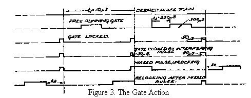
The speed with which locking can be obtained is a function of the gate width and the rate at which the gate pulse drifts with respect to the desired pulse train. This locking speed will be maximum for any given gate width, when the drift is equal to one whole gate width per period. Two conflicting points arise when the drift rate is considered. If we assume for a moment that the selector is already locked to the desired pulse train and that the drift rate was zero, then it would not matter how often or for how long the pulse disappeared, it would always reappear at the right place and there would be no delay in looking on. In order to obtain zero drift perfect stability would of course be required. If there was zero drift and locking had not occurred, then it would never take place. As the drift rate is increased the number of pulses that can be missed before unlocking occurs will grow less, so also will the time taken for relocking to occur. Figs. 1 and 2 illustrate what happens with two different rates of drift.
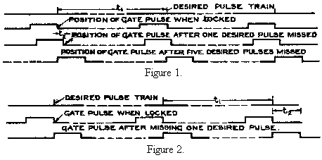
The time taken for relocking after desired pulse has been missing long enough for unlocking to occur is equal to t1 x 2/t2 where t1 = time in secs. between desired pulses and t2 = amount of drift per period, expressed in seconds.
It will be worth while here to consider a few examples. With a P.R.F. of 100 cps t1 = 10-2 secs. Using a gate pulse 50 µS wide and making t2 = 10 µS five pulses would be missed before unlocking occurred, it would then rates of drift take 10 secs to relock. Using the same gate pulse width but making t2 = 50 µS would allow unlocking to occur when only one pulse was missed, but it would relock in 2 secs, this is the minimum time for relocking when using this particular gate pulse width.
To be able to lock on in 0.5 sec. the minimum gate pulse width would be 250 µS, the drift rate would have to be 250 µS also, unlocking would therefore occur whenever a pulse was missed. For the particular job the selector was required to do it was decided that as long as it would never take longer than 0.5 sec. to lock on, it was relatively unimportant if one missed pulse caused it to unlock.
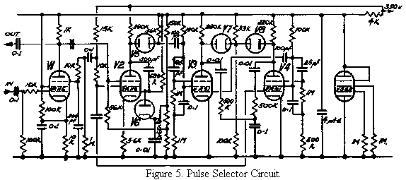
If the gate pulse was always 250 μS wide, too many interfering pulses would pass through the gate. This difficulty was overcome by making the gate pulse 300 μS wide and causing it to decrease to 50 μS when locking was obtained. This is done in the following manner. A time delay circuit, which operates for a time equal to t1 - 50 μS, triggers on a circuit which produces the gate pulse, normally 300 μS wide. The gate pulse is applied to the gate valve, and the gate valve coupled back to the gate pulse producing circuit in such a manner as to trigger it off immediately a pulse passes through the gate valve; the time delay circuit is started when the gate pulse circuit is triggered back. This automatically gives a drift rate of 250 μS per period since 250 μS are added to t1 if no pulse comes through the gate.
The sequence in absence of any pulse is briefly:- Stage one, delay circuit starts, runs for t1 - 50 μS and then causes gate to open. Stage two, gate remains open for 300 μS and then shuts, at the same time restarting delay circuit.
With desired pulse present the sequence is:- Stage one, same as before. Stage two, gate remains open for 50 μS and is then shut by incoming pulse, as the gate shuts it restarts delay circuit.
With an interfering pulse preceding the desired pulse by, say 30 μS, the sequence is:- Stage one, same as before. Stage two, gate remains open for 20 μS and is then shut, and delay restarted by interfering pulse (desired pulse having no effect). Stage one is started 30 μS too soon so that Stage two is also 30 μS early, gate remains open for 80 μS and is then shut be required pulse which starts the delay again.
When a pulse is missed altogether the sequence is:-Stage one, delay runs for t1 - 50 μS, gate opens, Stage two, gate remains open for 300 μS shuts, starts delay. The next stage one starts 250 μS late, missing desired pulse, selector is now unlocked. After a number of pulses equal to t1/t2 - 1 selector will again relock. These operations are all illustrated by Fig. 3.
It will be noticed that the effect of an interfering pulse (when it comes into the gate) is to prevent the required pulse from passing through the gate. An interfering pulse replaces the desired pulse and does not add to it, in its effect on the circuits fed by the gate.
The delay period (t1 - 50μS) cannot very well be determined by a normal oscillator circuit since it has to remain quiescent for any time between 0 and 300 μS once per cycle of the P.R.F. The method adopted was a valve delay circuit of the Miller feed back type.
The Delay Circuit
This circuit is a modified form of the screen coupled
Phantastron.
In this the actions of the "Phantastron" and the "Transitron" are combined in one valve. When switched on the normal transitron action, assisted by the positive feedback to the screen from the anode-control
grid coupling, starts the circuit up.
Starting from a point when the screen current has forced the suppressor down to a negative voltage large enough to cut off the anode current; the action is as follows. The suppressor voltage will become less negative as the capacitor C2 discharges through the resistor R4. When it reaches the point at which anode current starts to flow, then by normal transitron action, screen current will begin to fall; this will be greatly assisted by the falling space current due to the normal phantastron action (falling anode voltage fed into control grid). There is now a very rapid switch-over to the conditions necessary for Miller rundown of the anode voltage (screen voltage high, keeping suppressor up and anode current on). When the anode bottoms the control grid voltage will rise, increasing the space current, which will go to the screen thus pushing the suppressor down, cutting off the anode current and hastening the switch-over to the original condition.
The addition of R5 (with C3 to pass the sharp edge of the screen waveform) limits the suppressor current and lowers the negative mean of the suppressor waveform. This prevents premature cutting off of the anode current by the falling screen volts. The waveforms are shown in Fig. 4. The anode rundown can be initiated at any time after the anode voltage has been caught by the diode; this can be done by applying a fairly large pulse to the suppressor grid or a small negative pulse to the control grid.
If care is taken, the time taken by the anode run down can be made almost completely dependent on the product of C1 and R1.
If a silver mica capacitor is used for C1, and R1 is made up of high stability carbon, and nichrome wire wound resistors, in the proportion of two carbon to three nichrome, the temperature stability will be quite high. A test was made on the original model in which the temperature was changed by 40°C and the supply voltage changed ± 10%, the greatest change in delay was less than 0.5%.
The recovery time of the circuit cannot be made short enough to enable the delay to be repeated within the necessary short interval (0.300 μS). The difficulties attached to this are overcome by operating two similar circuits in series, each one running for half the delay period, giving half the period for recovery, which is ample.
The Complete Circuit
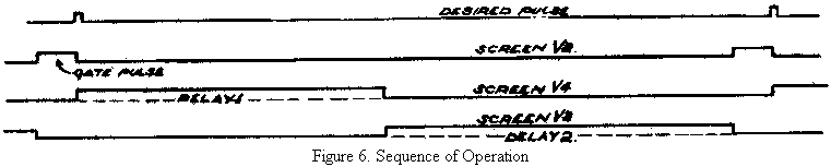
This consists of two VR1161 two VR91, and two VR541 type of valves, and a VS68 voltage stabiliser. The circuit, and sequence of operation is shown in Figs. 5 and 6.
V1 is the gate valve, the mixed pulse trains are applied to the control grid, the gate pulse to the suppressor grid, the 10K resistor and 200 pF capacitor on the suppressor grid is to delay the closing of the gate for about 6 μS. thus allowing pulses up to this width through.]
V2 and associated components is the gate pulse circuit. This is a normal phantastron circuit adjusted to run for approximately 300µS (this period does, not need to be accurately defined, since it only determines the drift rate). It is triggered on at the end of the delay period by differentiating the negative going edge of the V3 screen pulse and applying it to V5, the anode catching diode. Triggering off is done by the negative selected pulse appearing on V1 anode. This pulse is applied to the suppressor grid of V2 and, by cutting off the anode current, arrests the run down, thus producing the same negative edge at the screen as would normally appear at the end of the run down. The division of the screen resistors is made in order to keep the loading on the screen as light as possible. This is necessary because of the possibility of an interfering pulse getting through the gate immediately it is open and triggering V2 back immediately after it has been triggered on. The screen voltage must rise as quickly as possible in order that V4 may be triggered on by the negative edge.
V4. provides approximately one half of the delay period. It is triggered on by differentiating the negative edge occurring at V2 screen when it is triggered off (either at the end of its normal run down or when arrested by an incoming pulse). This differentiating is done by the 100 pF capacitor and the grid impedance of V4.
V3 provides the rest of the delay period and is triggered on by he negative screen pulse from V4 being differentiated into its grid circuit through the 100 pF capacitor. Its circuit is identical with that of V4 with the exception of the suppressor grid leak, which is 1 megohm instead of 500K. This, by making the natural periods of these two delay circuits different, prevents them running in step, instead of in series as they are required to do.
Timing the selector is done by adjusting the value of the feed back capacitors of V3 and V4 to give approximately the required delay, and by making part of the 500K grid resistor of one of the delay valves adjustable, to give a fine control. The delay of these two valves should be kept approximately equal in order to give each one time enough for recovery.